From interest in outer space to the world of electron microscopes
Hitomi: My university major was in the electrical engineering field, where I studied plasmas. My specific research was on plasma thruster of rockets in outer space. A plasma is an ionized gas. The trick is how to control the plus ions and minus electrons. Already while in university, I made an academic society presentations about plasma applications to space, as I had a strong interest in outer space. The problem, though, is that whenever I started thinking about space, I would get so scared I could hardly sleep [laughs].
In studying how to control plasmas, besides application to engines that efficiently transmit power, I found myself becoming interested in other fields as well, such as processing by electron beams, and electron microscopes that use an electron beam to observe very fine objects. So when I completed the master’s program and was thinking about a career, I looked for a company doing research on electron beams and electron microscopes, and that’s how I encountered Hitachi.
Araki: I’ve been fascinated with space since childhood. It started when I went to a planetarium for the first time. Enchanted by the starry sky, I became a regular visitor and dreamed of becoming an astronomer. After I became a junior high student, though, I began having doubts about making a living as an astronomer and thought it might be safer to choose a different line of work. Then in high school I found out there was a field called materials engineering, and that it was a field of study relevant to a wide range of areas, from architecture and civil engineering to tiny things like semiconductors, so I thought I should be able to feed myself in such a career [laughs]. I also held out the hope that with luck, I would be able to study materials related to space.

In university, I was assigned to a materials engineering lab related to ceramics. Working in a lab that let us conduct research freely, I discovered the lure of experimentation and research, and came to feel it would be nice to have a research job in the future. Some of the graduates from the same lab worked in Hitachi and wereengaged in exciting R&D in the materials field. Learning about this was the occasion for my deciding to join Hitachi.
Coming to the same electron microscope research along different pathways
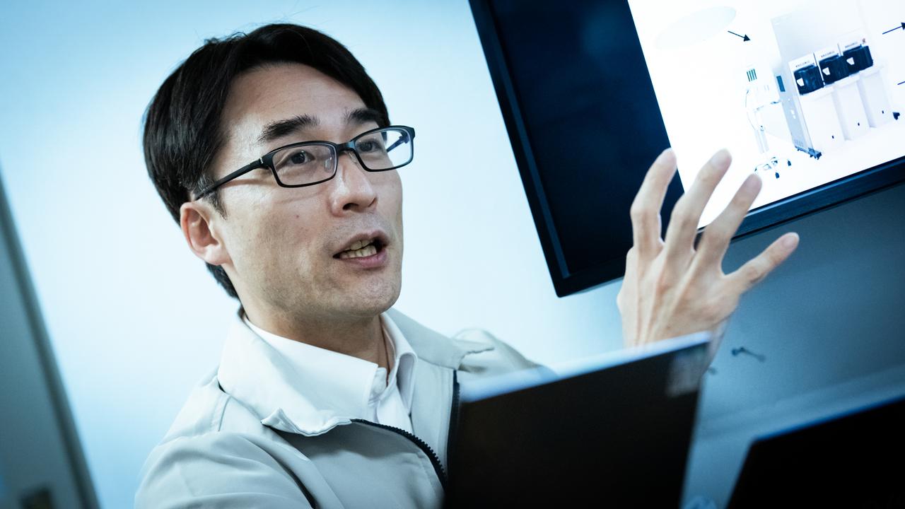
Hitomi: I entered Hitachi in 2005, and then spent the next five years conducting research on electron microscope applications. The usual image people have when they think of electron microscopes is of something for minutely observing materials or living organisms, but what I did was make applications targeting semiconductor manufacturers and others, for using electron microscopes to inspect and measure semiconductor circuits, making sure they have been made accurately according to the aimed-for dimensions. Since the electron microscopes were used to measure semiconductor circuits, from the start there were contacts with customers like semiconductor manufacturers.
After that, for around four and a half years starting in 2010, I was engaged in joint research on semiconductor manufacturing applications, at an IBM semiconductor R&D center, getting the chance to work with people from around the world involved in semiconductor manufacturing. Upon returning to Japan, at Hitachi High-Tech, which manufactures and sells electron microscopes, I became actually involved in everything from product development to delivery. What I developed while there was the CG7300 CD-SEM (Scanning Electron Microscope).
Araki: My research upon joining Hitachi was on materials for perpendicular magnetic recording hard disk drives. It was from this time, in fact, that I was using SEM to evaluate materials. After that, I was involved in developing permanent magnets, made from an alloy of neodymium, iron, and boron, for use in automotive alternators and motors. Then I started researching materials used for SEM with Hitachi High-Tech. My involvement in materials-related work from the time I joined Hitachi was pretty much as I had hoped, and since I was using electron microscopes all this time as a user, I felt it was only natural that I would come around to doing materials research for CD-SEM.
Building CD-SEM with high precision and no inconsistency from one instrument to another
Hitomi: The CD-SEM used to measure pattern dimensions on semiconductor circuits is one kind of electron microscope, which obtains images by focusing electron beam on the material to be observed and detecting signals (electrons) emitted back from the material. Since large numbers of electrons are emitted from edge portions of the material with irregular shapes, if these can be detected the shape can be known and pattern dimensions can be measured.
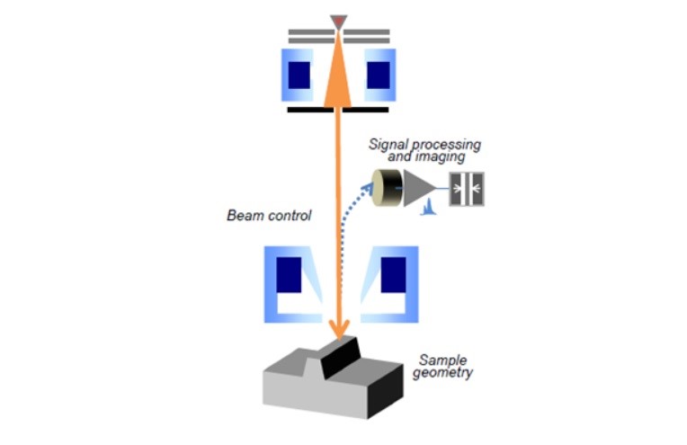
Conceptual drawing of CD-SEM structure and operation
The latest semiconductor devices today use pattern dimensions smaller than 20 nanometers (nano=10-9; 1 nanometer=1 billionth of a meter). The size of a hydrogen atom is around 0.1 nanometer, so what is needed is an instrument able to count the number of hydrogen atoms. This means an instrument using an extremely fine probe, with excellent spatial resolution, is necessary, while high stability is also essential. The test of a measurement instrument is its ability to achieve consistently high resolution. To this end, we have developed technology for controlling an electron beam with a beam using an electromagnetic field, as well as electrode and magnetic pole materials.
It was Hitachi, after all, that started the semiconductor CD-SEM business. Hitachi marketed the first CD-SEM in 1984, contributing to the measurement of semiconductor circuit patterns. For measuring semiconductor circuit patterns, CD-SEM is used as the standard yardstick; and Hitachi products incorporating the plentiful know-how Hitachi has built up for years continue to be used as the standard, maintaining the top global share to this day.
Meanwhile, semiconductors continue to make performance gains through further advances in scaling, or miniaturization. Semiconductor circuit patterns are formed by lithography, using light to imprint the pattern image on the semiconductor device. The shorter the light wavelength, the finer are the patterns that can be formed. The state-of-the-art lithography technology uses very short wavelength ultraviolet light, called extreme ultraviolet (EUV). Using EUV, nanometer-level devices began to be made in around 2019.
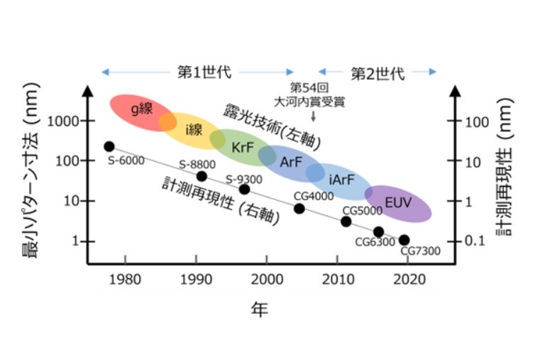
Trends in lithography technologies and measurement precision
At the same time as the capability for measuring such nanometer-class patterns has been needed, there has also been a demand for consistent data measurement by CD-SEM, minimizing to the extent possible any variability across different instruments. Increased production of semiconductors is leading customers to buy not just one but many CD-SEM instruments. If there is variability across these “yardsticks,” consistent measurement results cannot be obtained. The model we developed to embody the concept of what uniform hardware should be is the second-generation CD-SEM, CG7300.
What we had been asked to do is to please eliminate the difference between one instrument and another, down to 0.1 nanometer or less. There must not be more than a 0.1 nanometer difference between equipment A and equipment B. When customers want to make circuit patterns of 10 or 20 nanometers, they will generally tolerate a manufacturing variability of up to 10 percent of the target dimension. When a manufacturing variability of 1 to 2 nanometers is tolerated, if the CD-SEM deviation is 1 nanometer, manufacturing variability cannot be seen. If a difference between instruments of up to 10% of the manufacturing variability is allowed, the difference between instruments must be kept to an order of 0.1 nanometer.
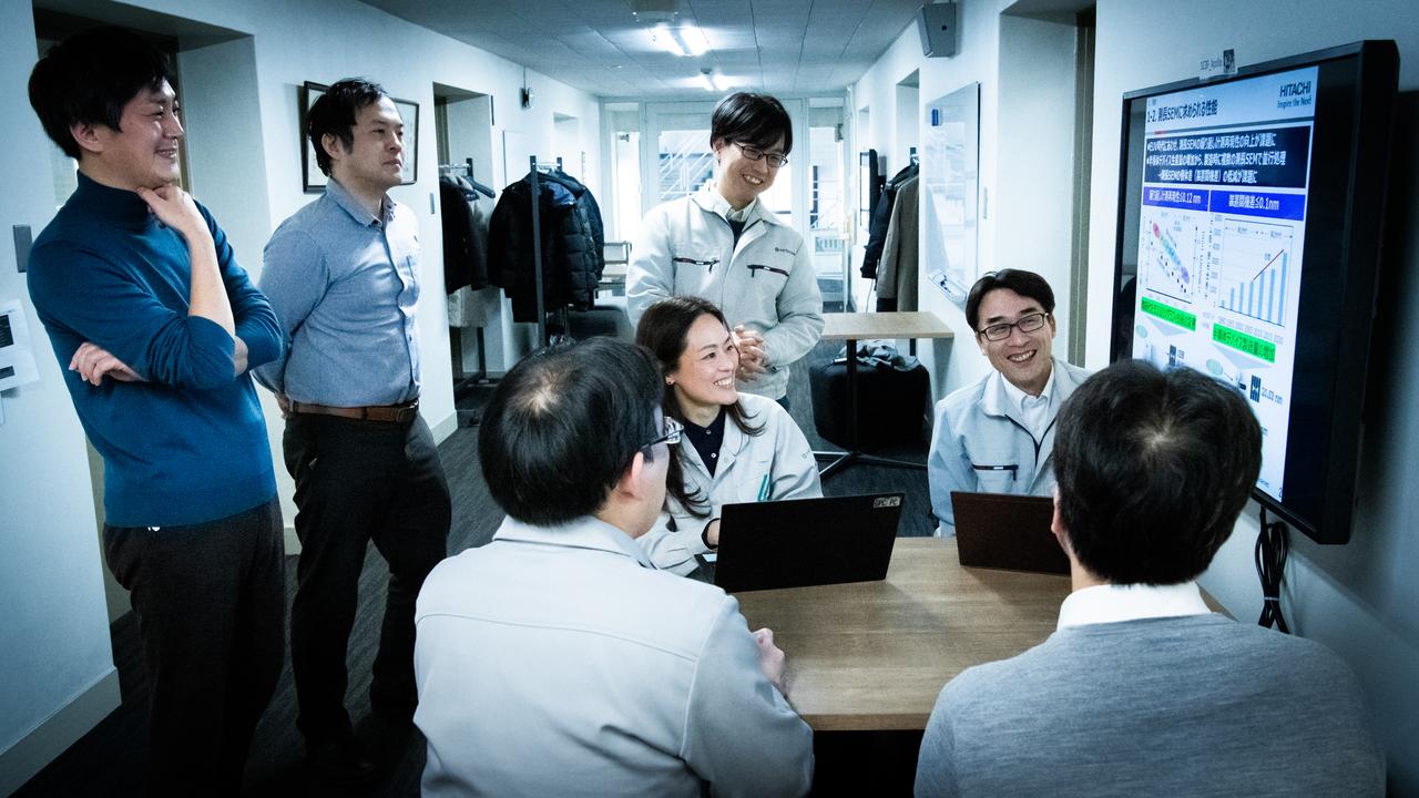
A CD-SEM measuring fine patterns formed on a semiconductor wafer. Members of the research team at the Instrumentation Innovation Center, taking on the challenge of developing the latest CD-SEM for use as a stable, high-precision “yardstick.”
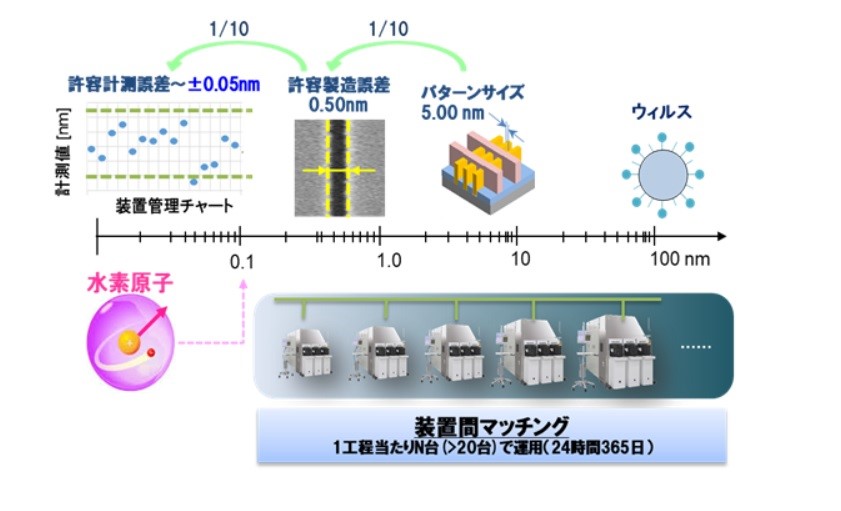
Upper limit of variability between dimension measurement equipment demanded in semiconductor device inspection
When you realize that 0.1 nanometer is the size of one hydrogen atom, it becomes clear even instinctively that the demands for deviation as a yardstick and for measurement precision are extremely high. As we carried out research on the factors causing differences across measurement instruments, and as to whether these differences could be eliminated by software tuning in case the causes could not be identified, we came up with a solid answer in the CG7300, successfully achieving commercial release in 2019.
When we developed the CG7300, the work of Araki-san was targeted at enabling stable electron beam control by making the hardware uniform. Since it would be difficult to reduce equipment variability to 0.1 nanometer by manufacturing skill alone, we also made use of digital technology for calibration.
Fully mobilizing all resources, from materials to comprehensive manufacturing, to raise the precision of the “yardstick”
Araki: My aim was to take a materials approach to making hardware that was all identical as a yardstick. In the case of CD-SEM, because of the need to measure the same things in the same way, it was all the more necessary to aim for the ideal of materials that were identical in every way. No matter how great the manufacturing skill, however, manufacturing error is inevitable, so the big challenge is how to reduce that.
Time limits are placed on the development team, who are faced with the demand to enable, within a short time, uniform-quality parts to be made, without manufacturing error. From a materials standpoint, you build the same part and evaluate each part, but you can easily end up spending a year or so in actually building and evaluating materials. Central to our research was how to condense that long process into a short time and achieve results efficiently.
What we thought of in addressing this was to incorporate a DOE (Design of Experiments), which is one kind of statistical method, for discovering an efficient testing method. Whereas normally you would have to build and evaluate materials by conducting tens or hundreds of tests, we figured out how to use statistical methodology in making and in evaluating materials, enabling the same yardstick to be made while minimizing hardware variability.
Hitomi: With a CD-SEM, an electron beam is focused on the material to be observed. The point here is how precisely the beam can be focused, and the development team put every effort into making the material that serves as the “lens” for this focusing. Customers wanted us to develop technology so that measurements could be carried out with no more than 0.1 nanometer variability between instruments, and the material developed by Araki-san greatly helped us meet that requirement.
Even so, the problem could not be solved by hardware alone. That’s why we created a standard for evaluating differences between instruments, measured the beam shape, and applied digital calibration technology, using software adjustments to make the beam shapes identical. This part was developed by software experts on the same team. The electron microscope is made up of many parts, including Araki-san’s materials development, electronic circuits and other hardware, and of course many different kinds of software. My own job is that of a producer, putting all the parts together and making sure the whole system is a piece of equipment that meets the customer’s desired specifications.
In addition to each of the individual technologies, by adjusting the overall system, we succeeded in keeping differences between instruments to within 0.1 nanometer for the CG7300. This is a 10% improvement over earlier models. Ten percent may seem like small progress, but in the 0.1 nanometer world, 10% has a big impact. Going from an error of 0.1 nanometer to 0.09 nanometer requires incomparably more effort than going from an error of 100 nanometers to 90 nanometers. Considering that the circuit dimensions of the semiconductor devices manufactured by customers are shrinking to 10 to 20 nanometers, I believe we did very well with this development.
This accomplishment was honored at the 69th Okochi Awards (2022) sponsored by the Okochi Memorial Foundation,* with Hitachi and Hitachi High-Tech winning the Okochi Memorial Production Prize for development and enhanced precision of a CD-SEM for measuring EUV lithography-generation semiconductors.
*The Okochi Awards are prestigious prizes given to outstanding individuals, groups, or businesses making major contributions to the advancement of science and industrial development, both in research and in implementation in production engineering, production technology, and production systems. The Okochi Memorial Production Prize is an award particularly intended to honor companies, factories, and other business entities.
Collaboration among researchers with different character types gives birth to results
Hitomi: Both in CG7300 development and in subsequent research, I have been working with Araki-san. Materials development is like a large chunk of know-how, not something that is often disclosed to the outside, nor does it involve active discussions with customers. As the interface with customers and the business divisions, I’m more visible and Araki-san is more in the background. She doesn’t let that bother her, though, as she carries on steadfastly with her development work; and that is what led to improvement of the basic performance of the CD-SEM. I feel that her qualities as a researcher really shine through in this respect. I’m more of an attention seeker, and the attention is what motivates me.
Araki: I have to respect Hitomi-san for his skill in pulling up onto the front stage basic and unobtrusive work done by those of us behind the scenes. [laughs] I believe a major reason for the success of this work was Hitomi-san’s coordination ability, as he was able to see the entire project and put it all together. What’s more, his role went beyond that of a coordinator to being someone who got us to notice small but important details. For someone like me, working mainly on hardware R&D, we wouldn’t see or hear much about the software side. As we tended to lose sight of the connection between the two sides, Hitomi-san would shine daylight on things with a view of the whole, pointing out precisely where a link was missing. I believe it was thanks to such a presence that the overall equipment was properly built, and also why it won an award.
Hitomi: As someone who even calls himself a “researcher specializing in communication,” I appreciate Araki-san’s kind words, but at the same time I feel I should be doing a bit more actual “research.” Still, I think it is necessary to have someone who, more than actually doing the research, connects the information learned and is able to make judgments as to what is important and what can be done; and I feel such a presence led to the success of the CD-SEM.
Keiichiro HITOMI
Unit Manager
Center for Digital Services
Nano-process Research Department, Instrumentation Innovation Center
Center for Digital Services, Research and Development Group Hitachi, Ltd.
Learning the importance of listening to the words of others
The Essentials of Governance by Wu Jing, a guidebook for good imperial governance in the Tang dynasty (Jogan seiyo, Japanese translation by Hiroshi Moriya, Chikuma Gakugei Bunko, etc.), made a big impression on me. As a book detailing the approach to governance of Li Shimin (Taizong), the second emperor of the Tang dynasty, it offers many things to learn about leadership. Among these is talk about three mirrors. It points out the value of using a bronze mirror for seeing your own appearance, using the mirror of history to learn from the past, and using people as a mirror to discern and correct your own mistakes. The people mirror is especially important, teaching us that we need more than “yes men” around us. Let me also mention one more book, Today and Tomorrow by automobile pioneer Henry Ford (Wara no handoru, Japanese translation by Kenichi Takemura, Chuko Bunko). Why do big companies exist? The book explains that this is to earn profits and make their employees happy. It made me aware that companies become profitable not just for the sake of profit but as something that is necessary to society.

Ryoko ARAKI
Chief Researcher
Center for Digital Services
Nano-process Research Department, Instrumentation Innovation Center
Center for Digital Services, Research and Development Group Hitachi, Ltd.
That human beings are part of nature should be seen as a warning
When I read Introduction to Natural Philosophy (Kodansha Academic Library) by philosopher Tomonobu Imamichi, whose long and distinguished career includes professorships at the University of Tokyo and other universities, I found it highly convincing on many different points. This book, published in 1993 when Japan’s “bubble economy” met its demise, suggests that perhaps “human beings should seek to learn more from nature.” Propelled by capitalism, human beings have continued to make use of natural resources as their own possessions; yet we are not the rulers of the Earth. The book sounds the warning that human beings are also part of nature and must care for nature. As we carry on with our work, our perspective can become quite narrow. At such times, reading this book makes me feel the need to find more room in my heart for personal comfort. Just as I thought about many things when looking at the starry sky as a child, even when engaged in my work, I would like to keep in mind the larger picture, and not let myself or the Earth be beaten down.