
Using machine learning, will contribute toward improved quality control and production efficiency
Hitachi has developed new image processing technology for semiconductor manufacturing processes, capable of high-sensitivity inspection of micro-defects of 10 nm*1 or smaller. Making use of machine learning,*2 the technology inspects extremely small defects with high efficiency by means of high-sensitivity defect detection and adjustment of the detection sensitivity based on the circuit layout. This technology will contribute toward improved quality control and production efficiency in the semiconductor industry.
Details of the developed technology are scheduled for presentation at SPIE Advanced Lithography + Patterning 2025, being held from February 23 to 27, 2025.
Background and issues
In the semiconductor manufacturing industry, growing demand for high-performance semiconductor devices is raising the importance of quality control in the manufacturing processes. Of particular importance for quality control is detecting defects, which directly impact product reliability and production efficiency. As the size of defects becomes microscopic, high-sensitivity defect inspection is demanded.
Technology details
In cooperation with Hitachi High-Tech Corporation, Hitachi has drawn on its knowledge and experience to date in such areas as image processing, machine learning, and data science to develop defect inspection technology having the following features, for use in semiconductor manufacturing (Fig. 1).
1. High-sensitivity defect detection technology using machine learning
The developed technology detects micro-defects from images captured by a scanning electron microscope (SEM), and has been confirmed to be capable of detecting with high sensitivity defects of 10 nm or smaller contained in evaluation samples. As pre-training steps for the machine learning, a large amount of data is generated consisting of images corrupted by adding noise to images of good products; then the features of data effective for reconstructing the good-product images from this data set are learned. In the actual inspections, good-product images are automatically reconstructed from the images containing defects; and by comparing images before and after reconstruction, microscopic defects as small as a few pixels are detected with high sensitivity.
2. Suppressing false positives*3 by adjusting detection sensitivity based on circuit layout
The increasingly microscopic size of defects to be detected makes it more difficult to differentiate between actual defects and manufacturing variability (non-defects), raising the issue of how to suppress false positives. To address this issue, technology was developed that uses machine learning to classify circuit pattern layouts. By adjusting detection sensitivity based on the layout, false positives occurring with certain types of circuit patterns is reduced. This made it possible to accurately differentiate between manufacturing variability and actual defects, suppressing false positives by 90% or more.*4
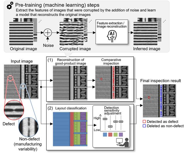
Figure 1: Using machine learning, (1) high-sensitivity defect detection technology and (2) technology for suppressing false positives by adjusting detection sensitivity based on circuit pattern layout
Future prospects
With this technology, Hitachi will contribute toward improved quality control and production efficiency in the semiconductor industry, and will support the stable provision of high-performance devices.
To contribute to promotion of digitalization and digital transformation (DX) in the manufacturing industry, Hitachi will continue to strive for advances in defect inspection and other image processing technologies.
*1 1/1 billion meters; 1/1 million millimeters.
*2 A method using algorithms to analyze vast amounts of data in a specific field and discover regularities and relationships among the data.
*3 Mistaken decision by inspection equipment that a normal location is defective.
*4 Numerical values derived from evaluation using evaluation samples.
For more information, use the enquiry form below to contact the Research & Development Group, Hitachi, Ltd. Please make sure to include the title of the article.
https://www8.hitachi.co.jp/inquiry/hitachi-ltd/hqrd/news/en/form.jsp


