
With the backdrop of a surge in semiconductor demand alongside AI advancements, as well as limitations of the conventional miniaturization approach, the industry is now entering a period of game-changing transition to chiplet technologies. Unlike conventional systems on chip (SoCs), which integrate circuits onto a single chip called a monolithic IC (single-die* integration), chiplet integration is a design and implementation architecture that separates the semiconductor die into multiple smaller ones (i.e., chiplets) on a function basis and combines them as one system using advanced packaging technologies.
*Die: A tiny piece (chip) of electronic circuit board formed on a wafer
Regarding the recent industry trend and Hitachi’s efforts, I interviewed three researchers, Yutaka Uematsu, Hiroaki Itsuji, and Soshi Shimomura, all of whom belong to Advanced Electronics Evaluation & Assembly Research Department, Green & Connective Innovation Center, Sustainability Innovation R&D, Research & Development Group, Hitachi, Ltd. (Uematsu: Principal Researcher; Itsuji and Shimomura: Senior Researcher)

Written by Kazumichi Moriyama (science writer)
Shift to chiplet-based semiconductor manufacturing using an open ecosystem
Backed by expanding needs, the semiconductor market is growing with a compound annual growth rate (CAGR) of approximately 10%. Meanwhile, miniaturization technologies, which have contributed to improving performance and reducing costs, are currently facing physical and economic limits. In logic fabrication with process nodes (generation of chip manufacturing technology) of 5 nm and below, the costs for mask sets and verifications are rapidly increasing, causing huge monolithic dies to lose their economic rationality. Even a shift to three-dimensional structures such as a fin field-effect (FinFET) transistor and a gate-all-around (GAA) transistor, which appeared as miniaturization progressed, leads to reduced yields and soaring costs due to their complexity. Besides, one basic fact is that an optimal process node varies depending on each functional block.
As a solution to these difficulties, chiplet integration in which small chips (chiplets) are fabricated on a function basis and consolidated into one package is attracting significant attention. If the function is divided into multiple dies, it is hoped to help improve the yield and thus reduce the costs. In addition, while high-performance CPU cores require advanced process nodes of 3 nm and below, input/output (I/O) and analog circuits with a mature node of 22 nm or 28 nm are advantageous in terms of characteristics and costs thanks to stable manufacturing. Thus, compared to a monolithic design in which these components need to be mounted with the same process node, the chiplet approach enables the use of nodes optimal to each function. Furthermore, chiplet integration also has the benefit of being capable of combining reusable semiconductor IP* components, thereby allowing the shortening of the development period, the expansion of product variations, and generation updates.
* Semiconductor IP (Intellectual Property) refers to pre-designed blueprints for specific chip functions such as CPU, memory controller, or the like
To sum up so far, a new packaging technology for combining separate functional dies fabricated with respective optimal processes (heterogeneous integration) has been presented as a solution to challenges associated with single-die designs, such as surging manufacturing costs and reduced yield.
Against this background, the chiplet packaging market for the semiconductor back-end process is experiencing a rapid growth with a CAGR of 42.5%. This indicates a shift from integration on a PCB to integration using more advanced packaging technologies.
Ongoing standardization for the open ecosystem
This transformation is accelerated by open ecosystem setups such as Universal Chiplet Interconnect Express (UCIe), an open high-speed and low-latency communication specification for connecting chiplets manufactured by different vendors, and the Open Compute Project’s Chiplet Data Extensible Markup Language (OCP CDXML), a data schema currently being standardized by the industry organization OCP. These standardization efforts, which facilitate the mixing of multiple companies’ chips, aim to drive a transition from the vertical integration model in which a particular company develops the entire system, to the open ecosystem in which an integrator combines various companies’ chiplets to construct an optimal system.
The governments of the US, European countries, Korea, Japan, and others are strengthening investments in back-end process and packaging technologies through the establishment of the CHIPS and Science Act (CHIPS Act) and the formation of consortiums focused on expanding semiconductor manufacturing. Therefore, the industry is transitioning from conventional miniaturization toward a new, standardized chiplet integration paradigm.
New unsolved issue: Silent data corruption (SDC)
The miniaturization and sophistication of semiconductors also pose a new issue related to reliability. One of the issues that have recently been highlighted is a system malfunction not sensed by the error detection mechanism, or data damage that occurs undetected, so-called a silent data corruption (SDC). Hyperscalers (major cloud service providers) have reported that SDCs inhibit AI training and cause erroneous inference results at datacenters, leading to a serious problem that impairs service reliability. “In the future, this problem may also affect automotive semiconductors,” Itsuji said.
According to a survey by Meta*, 66% or more of training interruptions occurred due to hardware failures, and in particular, approximately half of all failure cases are attributed to cutting-edge devices such as GPUs and HBMs (High Bandwidth Memory).
* How Meta keeps its AI hardware reliable - Engineering at Meta
However, since fundamental causes of SDCs lie throughout the supply chain, it is impossible to find the single cause to explain the phenomenon. Researchers have mentioned some possible causes, including cosmic-ray neutron-induced bit flips (soft error), sub-microscopic manufacturing defects, environmental factors such as thermal and operational voltage fluctuations, and cutting-edge device-specific failures caused by tight design margins when pushing performance to the limit.
Thus, there is a concern that the SDC, an already serious issue, will become further complicated and deepened if the open ecosystem for combining different vendors’ chiplets to build one system is widely adopted in the future. In such a case, unexpected failures and SDCs may often occur due to interactions between chiplets, making it extremely difficult to secure the reliability of the entire system. Therefore, the establishment of diagnosis and solution methodologies to overcome this challenge is an industry-wide open question left to the future work.
Hitachi’s inspection, diagnosis, and design technologies for ensuring high reliability
To address this reliability issue posed by chiplet integration, Hitachi takes an approach utilizing its long-standing technical capabilities as the core. In particular, based on implementation technologies and expertise in reliability evaluation that have been attained in the server and automotive sectors, the company positions the task of maximizing quality and reliability in the back-end process as its core strategy.
The first focus is on advanced inspection technologies. Hitachi High-Tech’s existing superior inspection and measurement technologies for the front-end process will be applied to the back-end process including packaging. In addition, to solve issues specific to new implementation forms such as a large-sized panel and three-dimensional stacking, Hitachi is developing a new inspection technology capable of evaluating microstructures even inside submicron-order (μm) connections.
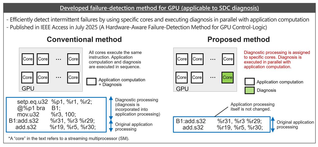
The second focus point is development of diagnosis technologies. Hitachi has developed a proprietary technique to diagnose GPU operations in real time as a methodology for guaranteeing the integrity of a single chiplet. By assigning diagnostic processing, which conventionally led to performance degradation, only to specific cores and executing the processing in parallel with the application computation, this has enabled efficient failure detection while suppressing a reduction in application throughput. Thus, it has become possible to efficiently detect certain control failures inside the chip that can lead to an SDC. This finding was published in IEEE Access in July 2025.
(A Hardware-Aware Failure-Detection Method for GPU Control-Logic)
Thirdly, Hitachi focuses on advanced packaging design and analysis technologies. In high-density chiplet mounting, advanced analysis technologies become essential. This is because issues associated with multiphysics, which involve interactions among multiple physical phenomena such as heat generation caused by current flow, influences on signal speed, package size, and thermal stress, become apparent. “With the conventional approach that performs independent design in each domain, it becomes nearly impossible to replicate interactions between the domains of a package close to physical limits,” Shimomura explained. For example, during substantial current flow, a considerable amount of Joule heat is generated. In advanced packaging designs, it is not possible to consider physical quantities such as heat and current flow in isolation.
Hitachi undertakes packaging design that factors in these complicated interactions by applying its existing analysis technologies that have been cultivated through the development of servers, storages, and other products. In addition, the company owns technologies for designing semiconductors for use under harsh environments such as on-vehicle electronics and power devices. These capabilities can be utilized to improve packaging reliability, according to the researchers.
With the transition to chiplet integration, technologies for interposers, which serve as intermediate substrates for connecting multiple dies, are also becoming important. Currently, silicon interposers are typically used, but low-cost alternative technologies are also considered promising due to silicon’s cost increase and other issues. Hitachi, which also owns a technology to effectively suppress noise specific to low-loss glass interposers (cavity resonance), is aiming to provide a design solution to achieving both performance and reliability. By integrating these technologies, the company is poised to contribute to developing high-quality and safe products to integrate into the open-system chiplet market and meet market needs.
Partnership and ecosystem strategies
Chiplet integration is not only an advanced version of a multi-chip module. It should be regarded as a comprehensive architectural transformation involving designs, interconnect standards, and electronic design automation (EDA) flows. It is a key technology and philosophy that can support the next-generation computing foundation by overcoming challenges with thermal design and interconnect standardization.
Recognizing that no single company can solve the challenge of assuring quality in the chiplet era, Hitachi is promoting its ecosystem strategies focused on collaboration with various partners in the industry through activities including participation in consortium research projects. The company aims to provide its own technologies as well as actively engage in a problem-solving platform common to the industry to improve the value of the entire ecosystem.
One such effort is Hitachi High-Tech’s participation in the JOINT3 consortium founded with the leadership of Resonac Corporation. The consortium brings together manufacturers of back-end process manufacturing equipment and materials. Through collaboration with manufacturers that ensure reliability and working across industries to tackle challenges throughout the entire manufacturing process, Hitachi aims to create solutions that no single inspection device can achieve.
In addition, Uematsu is a member of the National Institute of Advanced Industrial Science and Technology (AIST), engaged in research and development of fundamental technologies for chiplet interface designs for a national project and other programs. Leveraging expertise obtained through the industry-academic-government collaboration, the company plans to proceed with the standardization of the future open ecosystem and other collaborative work with diverse partners.
In any case, we have at least learned from the above that what is required for tiny chiplets is superior inspection technologies, advanced diagnosis and analysis technologies, and an overarching design philosophy for packaging these technologies at a higher level.
In various further growth business areas related to chiplets and advanced back-end processes, as well as in development work of core technologies to promote each business, Hitachi will hold the viewpoint of maximizing added value in collaboration with diverse partners, while playing a leading role in the ecosystem by exhibiting its own core strength in quality and reliability, operational technologies, and comprehensive capabilities.