The foundation for this cutting-edge semiconductor development actually lay in the analog-to-digital conversion circuit technology that Hitachi has refined over many years. Even in an era where semiconductor circuit research was gradually scaled back, dedicated researchers continued to persevere with studies in the field. Now, with the arrival of the physical AI era, this type of technology has become more important than ever. We spoke with Principal Researcher Takashi Oshima and Manager Yohei Nakamura of the Research & Development Group about the significance of Hitachi completing its proprietary edge AI semiconductor and the long journey of trial and error that brought it about.
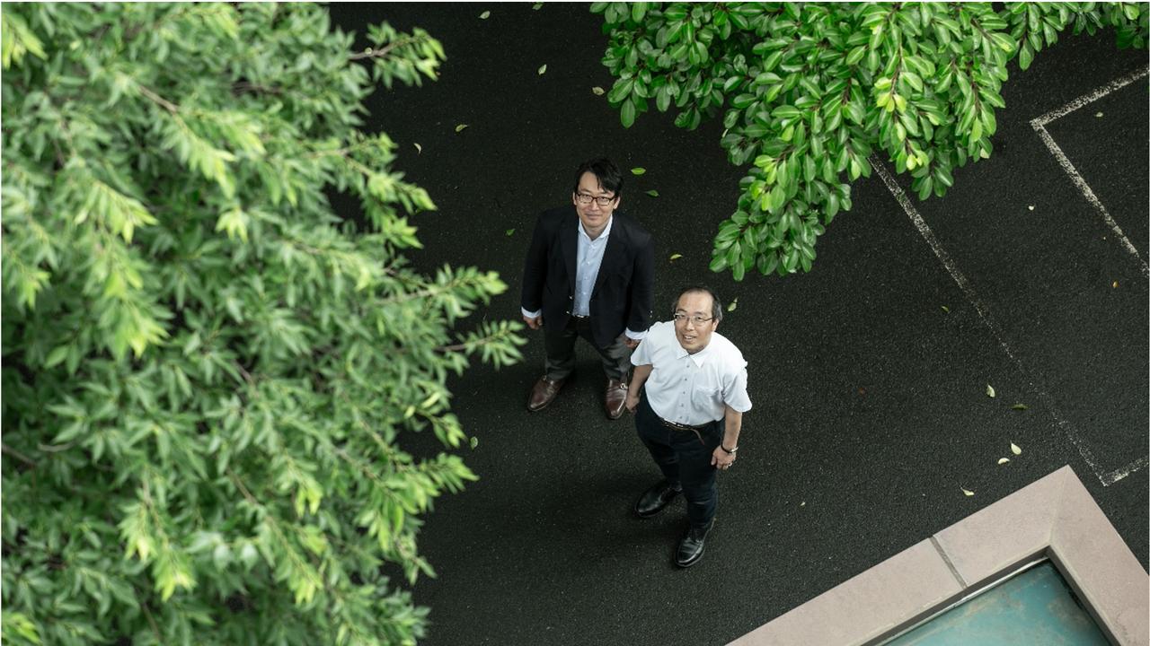
Two researchers striving to create tangible value
Oshima: I joined Hitachi in 2001, and I’ve been researching circuits and semiconductor chips since my days at the Central Research Laboratory. As a student, I majored in physics and pursued a doctorate with the aim of becoming a physicist. When it came time to find a job, though, I pivoted and went into circuit research. Although physics was certainly interesting, I probably made the switch because I also liked building electronic devices and radios and couldn’t forget that sense of joy and excitement I felt when something I built actually worked. But since my specialty was physics, I assumed it would be difficult to find a job in circuit research. It was around then that I learned that Hitachi’s Central Research Laboratory—today known as the Research & Development Group—was recruiting researchers in the field of analog circuits. I decided to challenge myself and apply, and fortunately, I was offered a position. I still remember how happy I was to join Hitachi.
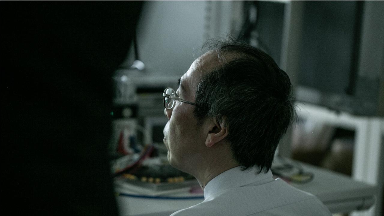
Takashi OSHIMA, Edge Computing Research Department, Sensing Integration Innovation Center, Sustainability Innovation R&D, Research & Development Group, Hitachi, Ltd.
I was involved in circuit design from the time I started working here, and I eventually saw some of that work through to commercialization. At first, I worked on developing integrated circuit (IC) chips compliant with the Bluetooth short-range wireless communications standard. In 2003, Hitachi’s Semiconductor & Integrated Circuits Group, which was leading development on those chips, merged with Mitsubishi Electric’s Semiconductor Group to establish a joint venture. For many years, I continued R&D on semiconductor chips in the joint venture’s portfolio as part of Hitachi’s Research & Development Group. It was at a time when Hitachi was gradually stepping back from semiconductor manufacturing.
Nakamura: I joined Hitachi in 2011. Oshima was in charge of my orientation and training, and he taught me the fundamentals of semiconductor circuits. In college, I studied semiconductors in the process of getting my electrical and electronic engineering degree; in graduate school, I worked on designing a chip based on neural networks modeled on the human brain. Although it was a small-scale chip with only one or two neural circuits, it was an extremely valuable experience. I considered pursuing a doctorate, but I wanted to help bring AI technology to life through chip design as soon as possible and put it to use in society—despite realizing how difficult it would be. That led me to pursue a career in private-sector research, which is how I eventually ended up knocking on the door of Hitachi’s research laboratories that conducted R&D on sensor circuits and semiconductor circuits.
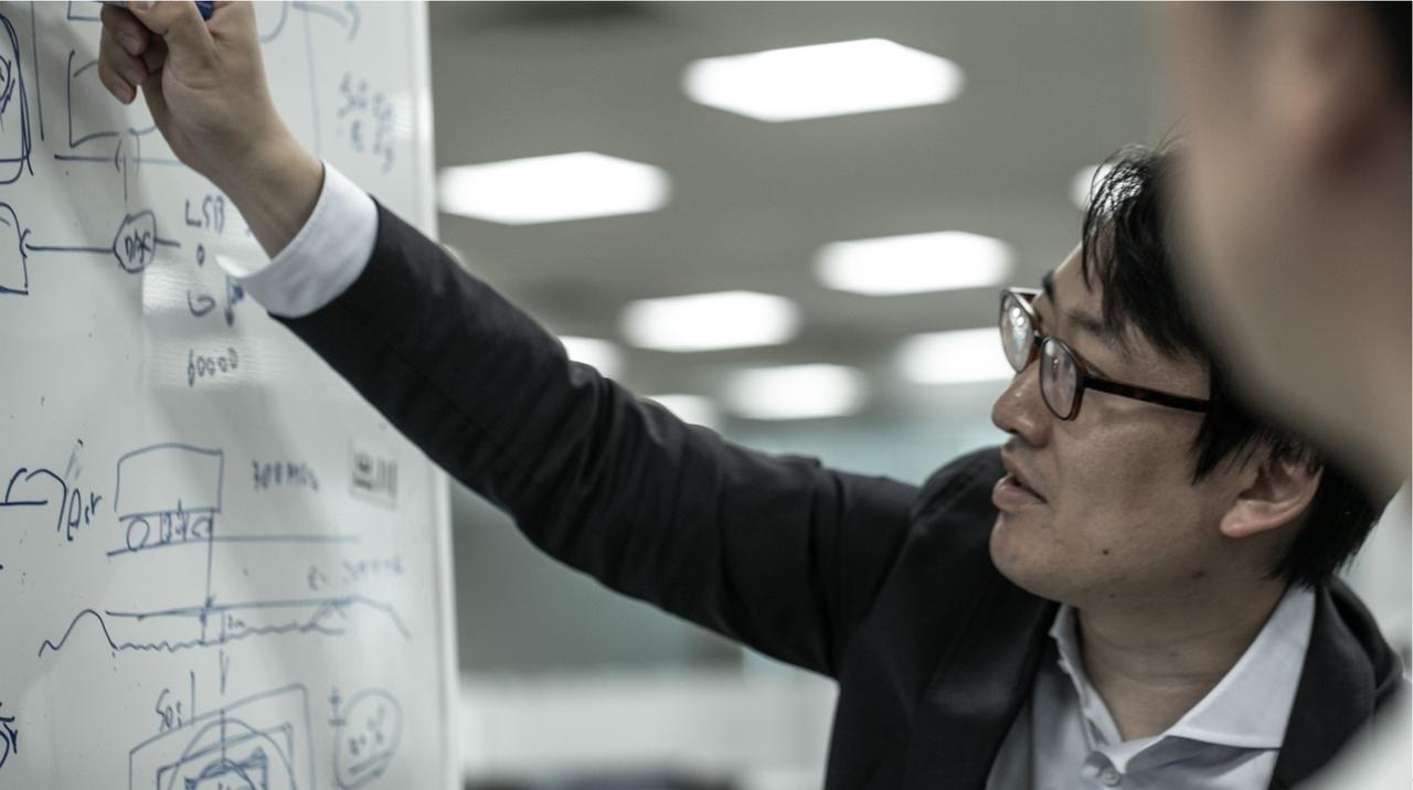
Yohei NAKAMURA, Edge Computing Research Department, Sensing Integration Innovation Center, Sustainability Innovation R&D, Research & Development Group, Hitachi, Ltd.
Upon joining Hitachi, I started researching new approaches for future semiconductors under Oshima’s guidance. Rather than developing large-scale integrated circuits (LSIs) themselves, my research focused on how to optimize the use of LSIs through data processing to enhance their performance. More specifically, I focused on applying digital processing technology to improve the performance of analog-to-digital conversion circuits. Oshima and I gave our first conference presentation on our research together in 2013. Later, in line with the Company’s move to spin off its semiconductor business, I shifted my research focus from semiconductor chips to the manufacturing side of LSIs, including developing circuits for semiconductor manufacturing equipment. I was later seconded to Hitachi High-Tech, where I continued pursuing R&D in the field up until three years ago.
Persevering with semiconductor chip research through difficult times
Nakamura: As Hitachi phased out its semiconductor business, it naturally scaled back its semiconductors research, as well. But still, Oshima continued to forge ahead with research into semiconductor circuits. When I returned to the Research & Development Group from Hitachi High-Tech, he was still working on the design process that would eventually lead to Hitachi’s proprietary edge AI semiconductor. I joined the project around that time, in 2020. While Oshima coordinated the technical aspects of the chip as lead researcher, I joined the project from an application perspective.
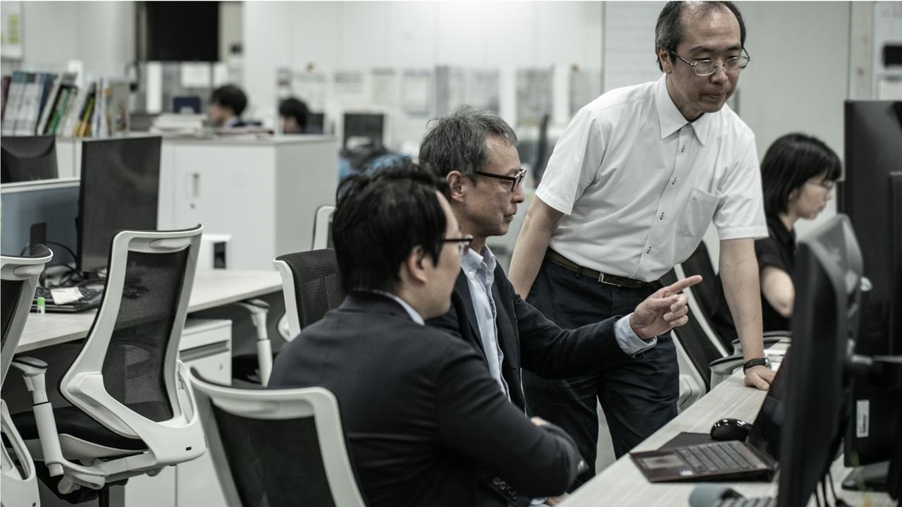
Oshima: Although I continued researching semiconductor chips after 2010, chip and circuit development represented only a small part of the research going on at the Hitachi laboratories. Until 2020 or so, it was hard to conduct large-scale development projects. At the same time, though, Nakamura helped us establish our strength in analog-to-digital conversion circuits after he joined Hitachi. By presenting our research findings at conferences and through other efforts, we were able to maintain our presence both inside and outside the Company.
And semiconductors eventually made a comeback: after those difficult times, semiconductors once again came to be viewed as a strategically important resource for Japan—and a boom in the semiconductor industry arrived around 2020, driven by the advent of AI. In that context, we were able to link the analog-to-digital conversion circuit technology we had kept working on to the development of edge AI semiconductors. One of the strengths of Hitachi’s Research & Development Group is that the Company’s expert researchers do not simply work independently; there is a strong emphasis on teamwork. In that sense, I was very fortunate to have Nakamura, with his expertise in circuits, join the team.
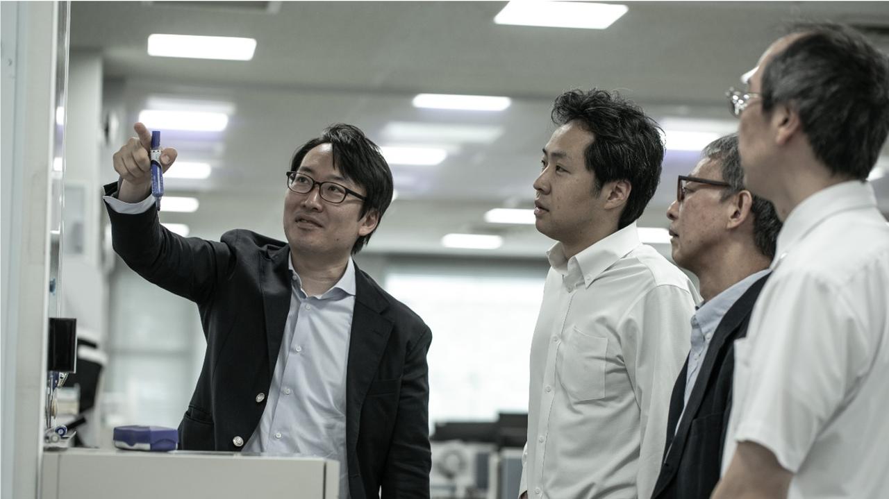
Nakamura: I’m always impressed by how Oshima approaches technical challenges head-on and tackles them right to the very end. That dedication and effort have enabled him to find a way forward and maintain a unique presence in the field. I really believe that Oshima’s commitment is the reason semiconductor circuit research continues at Hitachi today.
Analog-to-digital conversion circuits: Discovering a new way forward in the AI era
Oshima: Around 2012, deep learning began to deliver promising results, sparking renewed anticipation for AI technology. Around 2017, our managers and engineers began discussing whether there was a way Hitachi could utilize the chip and circuit development technology we had worked on to that point.
Nakamura: One event that probably accelerated these discussions was the 2019 establishment of the University of Tokyo’s Systems Design Lab (d.lab), a research center for semiconductor design that aimed to make it easier for companies and universities to develop advanced chips. Hitachi also joined d.lab, and we thought, “Since we have this opportunity, why not make something?”
This idea was passed on to Oshima, who had a vision to fuse our ongoing analog-to-digital conversion circuit research with AI chip development in line with the changing times. Although I wasn’t involved in the project yet at that point, we found that combining the developing technology with analog-to-digital conversion circuits also brought out the strengths on the digital side. That eventually led to the development of the proprietary edge AI semiconductor we’re introducing here.
Oshima: When we were developing the edge AI semiconductor that the Company announced in 2025, we didn’t know exactly what applications it might have yet. When we began development in 2020, all we had was an overall concept of developing a semiconductor that combined analog-to-digital conversion circuits with an AI chip. At the time, the AI field wasn’t dominated by generative AI as it is today—instead, image recognition using deep learning was one of the major topics of focus. But at Hitachi, we felt that in addition to innovations in AI processing itself, we should incorporate our strength in analog-to-digital conversion circuits into the chip design. The chip would take in sensor signals, convert them into digital signals using analog-to-digital conversion circuits, convert those signals into images, and then have the AI perform image recognition. Our hypothesis was that if we could convert analog signals from a range of sensors into images and have AI recognize them, the technology would have useful applications.
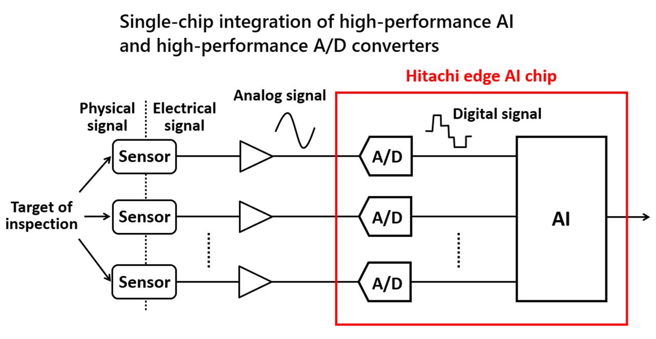
At the time, we were scrambling to put together a narrative that would convince management to support our development. We needed to clearly explain the significance of performing image recognition on analog sensor data. Looking back now, however, you can see that the idea of a chip leveraging analog-to-digital conversion circuits to have AI make decisions based on worksite data is exactly what physical AI is all about.
Nakamura: By the time I returned to the project, the technology had progressed considerably. Combining it with the analog-to-digital conversion circuits had brought out the strengths of the digital side, too. Hitachi’s proprietary edge AI semiconductor was beginning to take shape.
An energy-efficient AI semiconductor that brings intelligence to worksite equipment
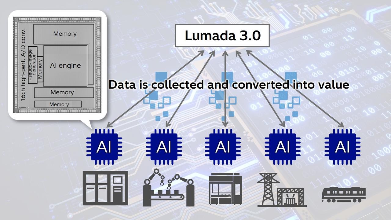
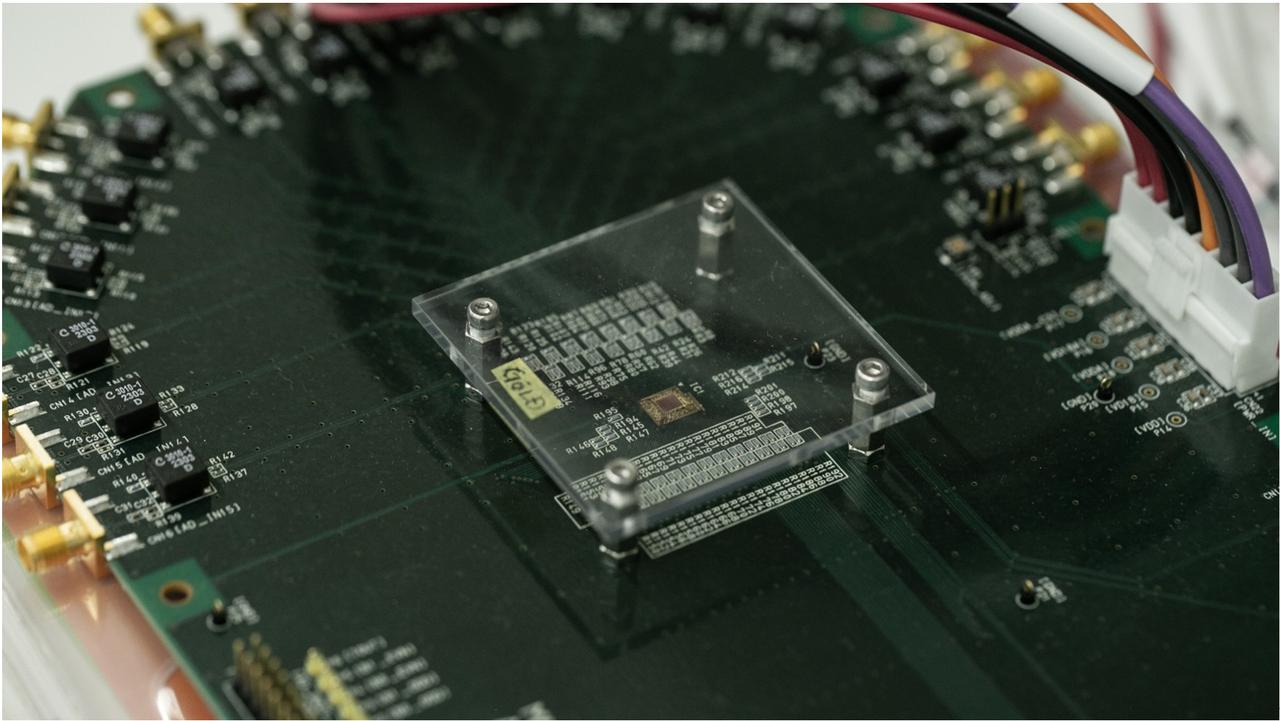
Oshima: Through these efforts, we were able to combine a high-performance AI chip and high-performance analog-to-digital conversion circuits into a single edge AI semiconductor. Hitachi’s edge AI semiconductor integrates 16 analog-to-digital conversion circuits on one side. An AI engine is at the center, surrounded by memory. The outputs from the analog-to-digital conversion circuits are converted into images by a pseudo-image generation circuit, which the AI engine then performs image recognition on. The input signals can be data from a variety of sensors, not just camera images. Converting signals from multiple sensors into images and having the AI engine recognize conditions and changes provides insights into the equipment or devices where the sensors are installed. In a single chip, we were able to integrate the functions for handling sensor signals as images and using AI to analyze the images.
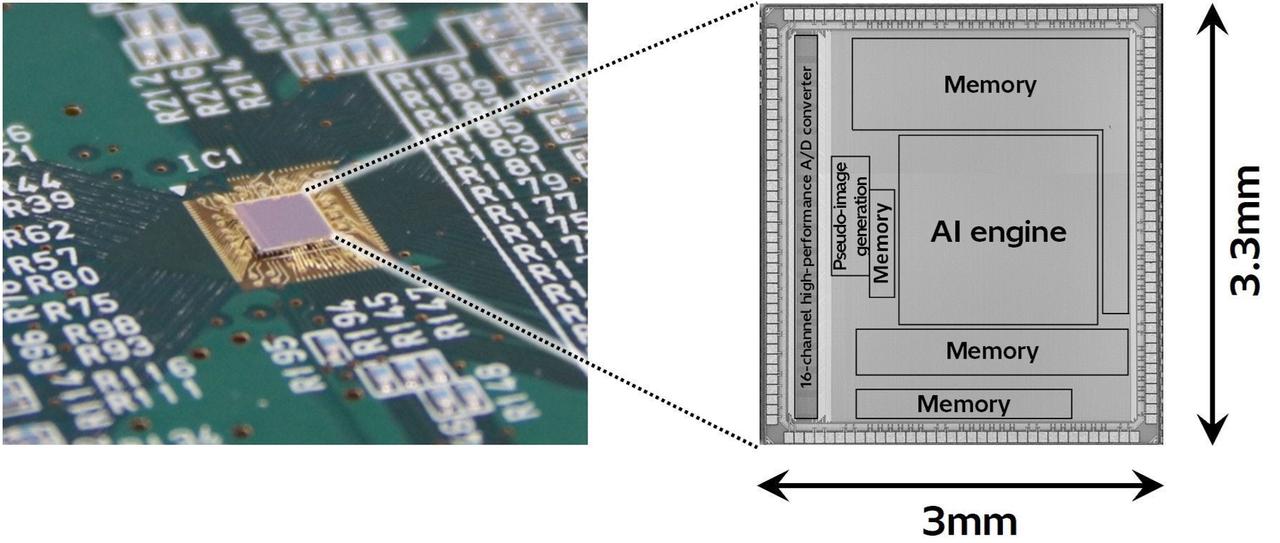
Detailed Structure of the Edge AI Semiconductor
Hitachi’s edge AI semiconductor has other important features, one of which is how it incorporates high-capacity on-chip memory. General-purpose AI chips, such as GPUs, devote a significant part of their circuitry to graphics processing, which serves as the AI engine. Because these processors were originally developed for graphics processing, they incorporate relatively little on-chip memory within the circuitry. When performing AI calculations, a lack of sufficient memory can cause a bottleneck in the supply of data, making it impossible to realize the full potential of a high-performance AI engine.
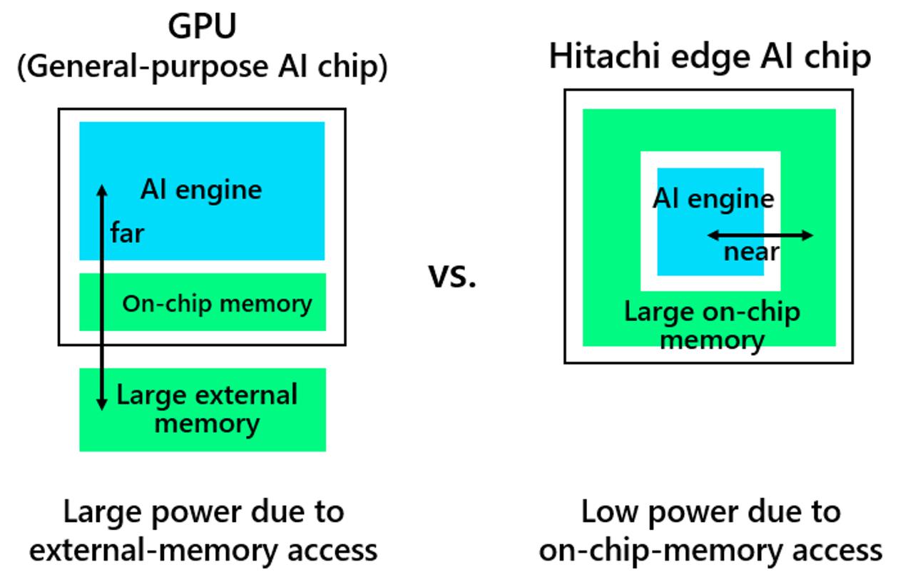
Our edge AI semiconductor incorporates high-capacity on-chip memory to balance the processing capability of the AI engine, which is optimized for image processing. This makes it possible to supply data to the AI engine without unnecessary delays. We also configured the high-capacity on-chip memory so that it surrounds the AI engine, a design that shortens the distance between the memory and the AI engine to help reduce power consumption. The edge AI semiconductor we ultimately developed achieved twice the AI processing speed of a GPU while consuming one-tenth the power or less. In other words, at the same power consumption, it delivers 20 times the AI processing speed.
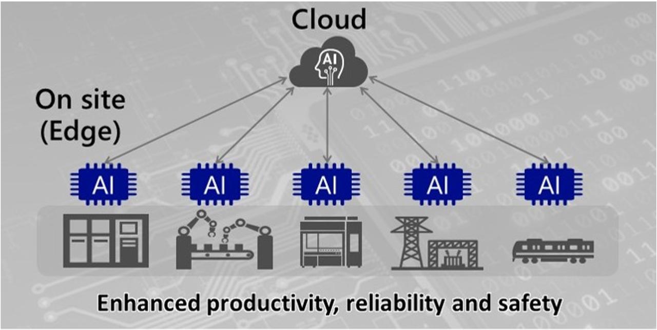
Low power consumption is a major advantage in deploying Hitachi’s edge AI semiconductor in worksite equipment to perform AI processing. Semiconductor inspection equipment, one of the intended applications for this technology, is a prime example of equipment that can benefit. Lower power consumption also reduces heat generation, meaning that users don’t have to devote as much space to cooling and heat dissipation. Being able to add AI functionality to equipment with limited installation space is one of the keys for utilizing physical AI in practical applications.
The production of our edge AI semiconductor uses a leading-edge seven-nanometer complementary metal oxide semiconductor (CMOS) process. We gained access to this state-of-the-art technology at a relatively low cost by utilizing the ecosystem of the Research Association for Advanced Systems (RaaS), which collaborates with d.lab. That said, manufacturing semiconductors via the seven-nanometer CMOS process is still expensive.
Developing AI for different sensors, equipment, and conditions used to mean designing separate algorithms for each case, as the sensors, the waveforms they output, and the conditions indicating abnormalities all differ from case to case. Hitachi’s edge AI semiconductor, however, converts sensor data into images, reducing the problem to one of image recognition. This makes it much easier to apply the algorithm across different sensors and types of equipment. As it turns out—or rather, just as we’d planned—this approach of converting data into images and training the AI proved capable of contributing to more efficient system development, as well.
Beyond technology: What is needed for practical application?
Nakamura: To be honest, I didn’t understand the value of this chip when I first joined the project. If even someone who had some experience with semiconductors—like myself—didn’t see that value, we would definitely not be able to communicate the value of our technology to other people. When an analog signal is fed into the edge AI semiconductor, it is converted into an image, and image recognition technology is then used to determine what condition the signal represents. However, I knew that people would struggle to understand the value of the technology unless they could actually see it in action. So I stressed the need for a demonstration unit, and I ended up being the one responsible for building it.
How could we demonstrate the operation of Hitachi’s edge AI semiconductor in a way that would communicate its value? As I thought about that question and got a deeper understanding of the chip’s underlying principles and internal structure, I began to realize, “This is a chip with tremendous potential.” I intuitively understood that, although there are GPUs that perform general-purpose AI processing, the value of our edge AI semiconductor lies in its ability to take in signals from sensors and other sources and have AI make decisions on the spot.
That led me to think about the types of applications we could use the edge AI semiconductor in to generate value. I started to ask myself why someone would want to have our edge AI semiconductor handle processing and development tasks that a general-purpose GPU could perform. One application I thought of was situations where data cannot be transmitted outside the equipment. When those constraints require AI processing to take place entirely within the device, the advantages of edge AI semiconductors—which are developed specifically to address power and heat dissipation issues—really shine through. Another great use case is mission-critical equipment that might need to continue operating for five or ten years after coming into service. General-purpose GPUs present supply-related challenges, as they undergo frequent updates, but proprietary edge AI semiconductors have the advantage of making it easier to control long-term supply.
Applications of the Edge AI Semiconductor Across Diverse Fields
Accordingly, we developed a strategy for selling more edge AI semiconductors by presenting a wide range of applications where those advantages could make a difference. We started by creating a list of all Hitachi High-Tech products, documented the processing that each device performs, and talked with people in the relevant departments to determine where Hitachi’s edge AI semiconductor could be integrated to deliver benefits. After reviewing our findings, we created a list of potential applications for the edge AI semiconductor. We began implementation with semiconductor inspection equipment and demonstrated that, even just among the Hitachi High-Tech products we reviewed, the edge AI semiconductor was capable of generating new value across many applications in the future. Although the effort wasn’t directly related to chip design, it was something I put considerable effort into.
Oshima: Nakamura worked so hard to persuade people throughout the organization, including management. Although our team believed in the benefits of the edge AI semiconductor, Nakamura’s efforts were critical in getting more people to buy in and convincing them that we were on the right track. His demonstrations showed how our semiconductors could be effective in semiconductor inspection equipment, I think, and his efforts to communicate potential applications of the technology in future products won more and more people over.
Hitachi issued the first press release on the development of the edge AI semiconductor in October 2025. At that stage, it was an announcement of an emerging technology still in the R&D phase. Then, in April 2026, the Company issued a joint press release with Hitachi High-Tech. It outlined an edge AI semiconductor with the potential for implementation in Hitachi High-Tech products, and the fact that the release was issued jointly with a Hitachi Group company highlighted that the Company was also placing strong emphasis on commercializing the technology. Moving beyond the technology that the Research & Development Group has developed, we are currently in the phase of getting quality assurance and other key elements for commercialization in place as quickly as possible to transform the technology into a product. We will also continue to advance R&D on edge AI semiconductors for industrial equipment.
Nakamura: To integrate the technology into products and bring it into the world, we need to move to the next stage and actually run it in environments where people outside the research laboratory can see it in action. Commercialization also requires building an organization capable of setting up a mass-production system and putting other necessary infrastructure in place. I want to commercialize this technology as soon as possible and have people see for themselves what our edge AI semiconductors can do. We will also keep working to communicate the value of the technology itself through international academic conferences and other channels.
LSI research in Japan has been on the decline for a long time; the number of people working in the field has fallen, too. However, I hope that Hitachi’s persistent efforts can help revitalize Japan’s semiconductor industry once again—and that our development will help spark renewed interest and activity across the country.

Yohei NAKAMURA
Manager
Edge Computing Research Department,
Sensing Integration Innovation Center,
Sustainability Innovation R&D
Research & Development Group, Hitachi, Ltd.
Learning from history: Turning promising technologies into products and businesses
I learned a great deal from Hitachi no zuno (The brain of Hitachi) by Katsumi Kato (Kodansha). My supervisor gave me the book when I began conducting R&D on LSIs. It tells the story of how Hitachi’s electron microscopes have evolved. My research had absolutely nothing to do with electron microscopes, so I was a bit puzzled as to why I’d gotten the recommendation. When I returned the book, my supervisor asked me what I thought of it. I didn’t have a good answer, so he sent me back to read it again [laughs]. Upon rereading it, I came to understand that while you can’t sell electron microscopes in large volumes, applying electron microscope technologies to semiconductor manufacturing significantly expanded the market. Through that historical lens, I got a true sense of how you can transform technologies into products and businesses. It was a valuable learning experience for me. I never got around to returning it to my supervisor, and it remains one of my favorite books to this day.
Takashi OSHIMA
Principal Researcher
Edge Computing Research Department,
Sensing Integration Innovation Center,
Sustainability Innovation R&D
Research & Development Group, Hitachi, Ltd.
A difficult book to recommend—but one that left a lasting impression
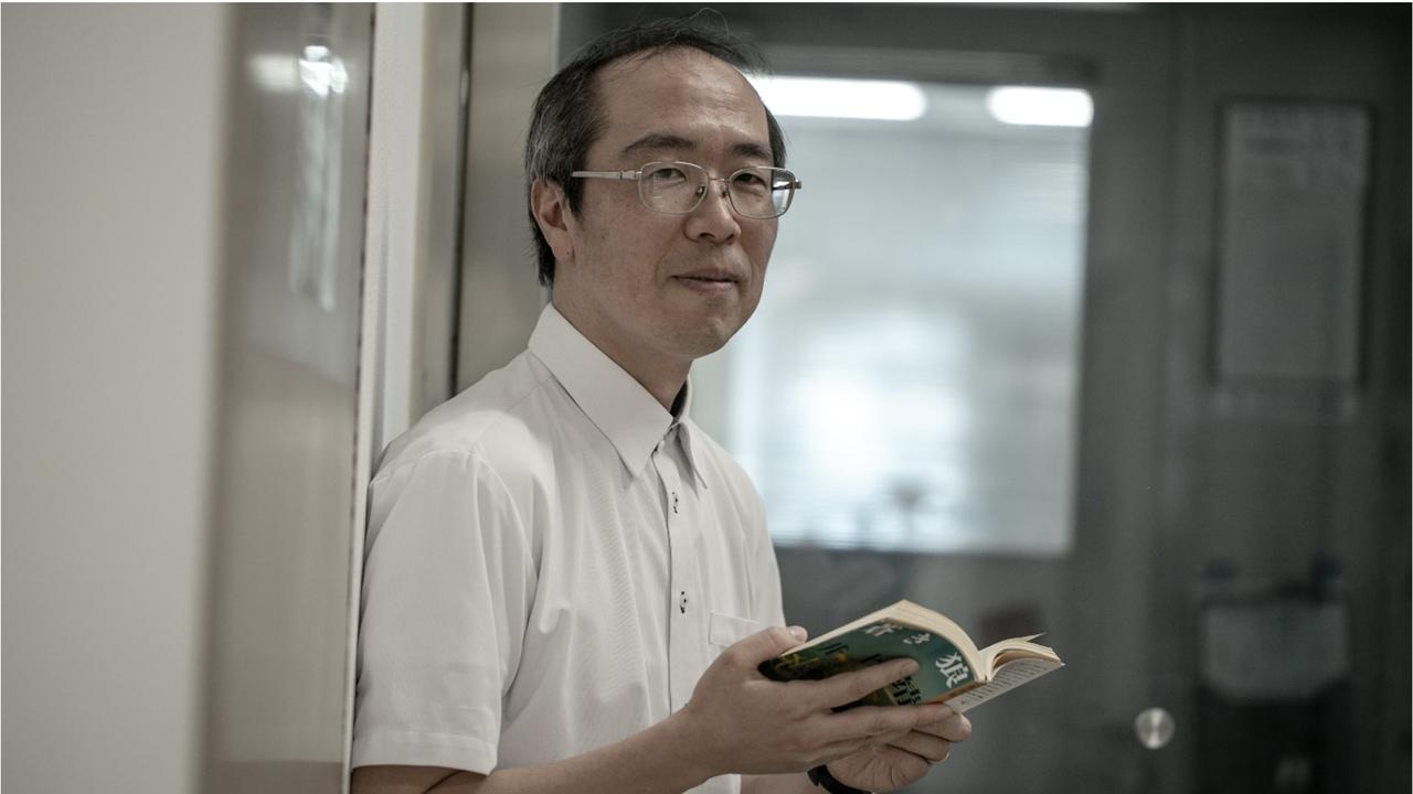
My pick is Aoki okami (The Blue Wolf) by Yasushi Inoue (Shincho Bunko). The story follows Genghis Khan as he expands the Mongol Empire and sets out to conquer the world. I read it when I was a child, and I’ve continued to reread it as an adult. It was written more than 50 years ago, and some of its depictions of slaughter and gender discrimination may be difficult for modern readers to handle. But I always find myself drawn back to it because I feel there are certain similarities between myself and the character of Genghis Khan. The way he pursues a single objective to the very end, his willingness to trust his allies and key figures as he moves forward—that resonates with my own experiences in some ways. There are many passages that make me feel uncomfortable or want to push back, so I would not exactly “recommend” this book. However, it evokes complicated feelings in me because there are traits of the character I identify with and feel drawn to.

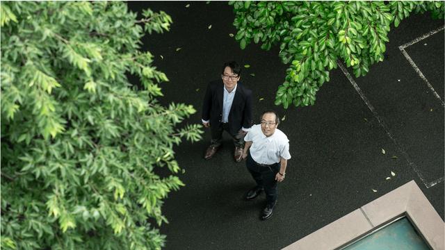
(Photo by Kiyono Hattori)